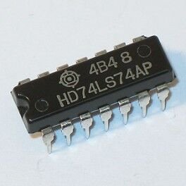
CD4011 NAND gates provide the system designer with direct implementation of the NAND function and supplement the existing family of CMOS gates. All inputs and outputs are buffered.
Your email will be used for sending Abandoned Cart emails
TC4011/ CD4011 – CMOS Quad 2-Input NAND Gate IC (Pack of 5)
-64%
Propagation delay time = 60 ns (typ.) at CL = 50 pF, VDD = 10 V
Buffered inputs and outputs
Standardized symmetrical output characteristics
Maximum input current of 1 ?A at 18 V over-full package temperature range; 100 nA at 18 V and 25?C
100% tested for quiescent current at 20 V
5-V, 10-V, and 15-V parametric ratings
Noise margin (over full package temperature range:
1 V at VDD = 5 V
2 V at VDD = 10 V
2.5 at VDD = 15 V
Volume Discounts- Buy More Save More! Discounts upto 20%. Contact us
Special Bulk Discounts for colleges, Schools, Companies & resellers Contact us
4 in stock
4 in stock


Reviews
There are no reviews yet.